Researchers have managed for the first time to grow p-type nitride semiconductor layers on zinc oxide substrates, enabling the creation of two sets of diode devices with light emission at two wavelengths (near-UV and yellow, green and blue) [Gon Namkoong et al, Appl. Phys. Express, vol3, p022101, 2010]. Previous attempts to grow p-type semiconducting nitrides have foundered on the volatility of ZnO and compensation of the p-type characteristic by oxygen migration into the nitride layers.
In the new research, low-temperature (500-550°C) molecular beam epitaxy (MBE) was used to grow nitrides on Zn-face ZnO substrates produced by Georgia Institute of Technology spin-off Cermet Inc of Atlanta, GA, USA. Gon Namkoong, the corresponding author on the research, is based at the Old Dominion University (ODU), Norfolk, Virginia. Other participants come from Georgia Institute of Technology (GaTech), State University of New York at Buffalo, Korea University, and substrate maker Cermet.
A 50nm layer of In0.07Ga0.93N was followed by 0.4μm of p-GaN (Mg-doped to hole concentrations of 3-5x10¹⁷/cm3). Both layers were produced using 'metal-rich' conditions. The substrate, as delivered, had an electron concentration of 3x10¹⁶/cm3. A comparison nitride semiconductor LED on sapphire was also produced with 0.15μm Mg-doped p-GaN (3x10¹⁷ holes/cm3) on 1μm silicon-doped n-GaN (1x10¹⁸ electrons/cm3).
Photoluminescence (PL) and electroluminescence (EL) studies were carried out. First electronic characterization of the diode properties shows an increased (~4x) forward current for a given voltage, comparing the nitride-on-ZnO with the nitride-on-sapphire device. However, blocking of the reverse current is not as good in the hybrid III-N/ZnO device. The forward current is enhanced with the ZnO substrate, both by its greater electrical and thermal conductivities. Sapphire is insulating and has a poor thermal conductivity.
The EL spectra of the hybrid ZnO/nitride LEDs show two main peaks (Figure 1) at high currents (60mA): one at 396nm (near-UV) and the other at 500nm (yellow). A weak peak at 483nm (blue) is also observed. Energy-dispersive spectroscopy (EDS) suggested that the blue peak was due to interdiffusion at the InGaN/ZnO interface, in particular deep acceptor states from Zn that has migrated into the InGaN layer. The near-UV is attributed to band-edge emission of the InGaN material. There is also band-edge emission in the GaN layer at 360nm.
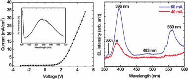
Figure 1: I–V characteristic (a) and EL spectra (b) of p-GaN/In GaN/n-ZnO with different forward currents. Inset of (a) shows photoluminescence of p-type GaN/InGaN/ZnO structures measured at room temperature. Peaks at higher current are attributed to emissions from the GaN band-edge (360nm), InGaN band-edge (396nm), Mg-related defects (560nm), Zn deep-acceptors in InGaN (483nm).
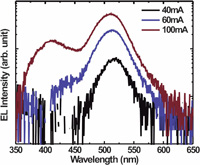
Figure 2 (above): Electroluminescence spectra of
p-GaN/In0.14Ga0.86N/ZnO LEDs
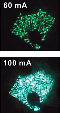
Figure 3 (below): photographs of the LEDs at different forward currents.
Further devices were grown with higher indium contents (In0.14Ga0.86) that gave blue and green emissions (Figure 2).
The 516nm green emission was dominant at 40mA. The green emission was attributed to Zn-related band emission in the InGaN layer. At 60mA and 100mA, a shorter-wavelength peak appears that blue-shifts from ~432nm (2.87eV) to 411nm (3.01eV) with increasing current. Non-optimal growth conditions are a likely source of non-uniformities of the emissions seen in Figure 2(b).
The researchers conclude that "multi-quantum well (MQW) structures in the active layer may produce bright dual wavelengths if impurities from the ZnO diffusing into the InGaN active layer are carefully controlled".
ODU and Cermet are collaborating to develop green LEDs with US Department of Energy funding. Namkoong, with researchers from GaTech and Wright State University (Ohio), has previously achieved impressive p-type doping levels of 1019 holes/cm3 in GaN by using a metal-modulation epitaxy (MME) molecular beam epitaxy (MBE) growth technique [Gon Namkoong et al, Appl. Phys. Lett., vol93, p172112, 2008]. Maximum hole concentrations achievable using Mg in normal GaN growth (MBE or metal-organic chemical vapor deposition) are usually in the range 1-2x10¹⁸ holes/cm3.
"Our current main focus is on defining growth technologies of III-nitride on ZnO substrate to reduce dislocation densities, increase hole conductivity, and control interfaces between III-nitride and ZnO substrates, which are key technologies to implement dual- or triple-wavelength light-emitting diodes," comments Namkoong on the future direction of the work. "We think that if multi-quantum well structures are used, instead of a single quantum well between p-type GaN and highly conductive ZnO substrates, it might be possible to produce brighter dual-wavelength light emissions," he adds. "In addition, since ZnO is an excellent luminous material — emitting various emissions including green, blue and even red wavelengths — the direct integration of III-nitrides on ZnO could produce white light-emitting diodes. Therefore, we have a vision to develop phosphor-free white LEDs. Furthermore, this technology can be a basis for green lasers with strong emission at 550nm and beyond."
In fact, Namkoong reports white LED emission based on this technology that is yet to be published.
Fuente:
Gerald Soto, CRF 2010-1.
No hay comentarios:
Publicar un comentario